Emerging semiconductors
We introduced foreign advanced semiconductor materials and high technology to continuously support the development of the domestic semiconductor industry and meet the increasing market demand.
CMP Polishing Pad
The CMP process is a combination of surface chemistry and mechanical grinding techniques to achieve micron/nanometer level removal of different materials from the wafer surface, resulting in nanometer level flattening of the wafer surface to allow the next lithography process to proceed.
View Details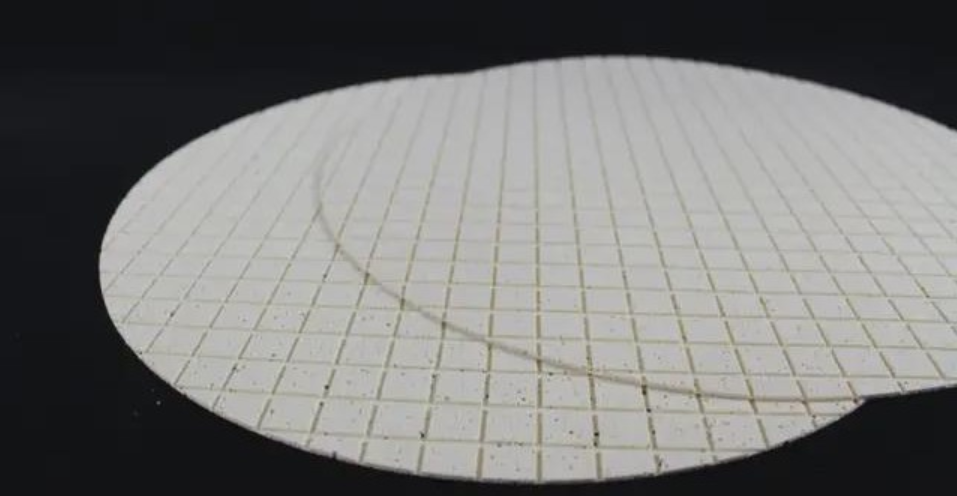
High-end Conductive Nonwoven Fabric Series
Based on LCP nonwoven fabric, it is a flexible conductive material processed by the continuous electroless copper-nickel plating, single/double side coated with conductive adhesive and release paper, featured by ultra-thin, highly conductive, electromagnetic shielding, die-cut adaptation, widely used in 5G base stations, flexible displays, TWS headphones and AI-powered computing temperature resistance.
View Details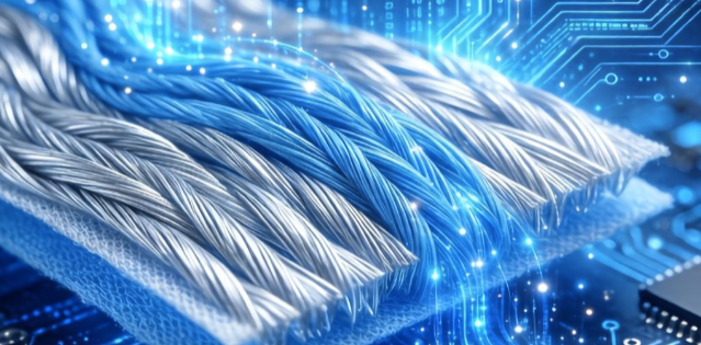
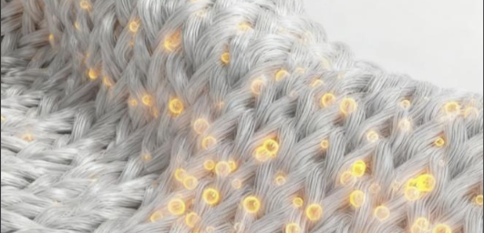
Conductive Fiber
High-performance fiber LCP as a base material, it is a functional fibers made by metallization modification (Cu/Ni/Ag plating) or carbon nanotube doping, comprising, and featured by high conductivity, antistatic, electromagnetic shielding, flexity and spinnability, for electromagnetic shielding and antistatic composite materials.
View Details